- PCB Engineering
- CAM Procedures
- Gerber File
- Gerber Generation
- Pick&Place Generation
- DFM Check Item
- DFM Check Details
- PCB FAB Tutorial
- Finished Surface
- Impedance Apply
- Impedance Type
- PCB Laminates|Stackup
- Stackup with Impedance
- Capabilities
- Tolerances
- Material Comparison Chart
- Rogers Matierl datasheets
- Rogers Material Choose
- Avoid missing Feature
- HDI PCB Stackup
What does Free DFM Check For?
Complete
ZIP Files
Inner Plane
Layers
1. Gerber
file for each copper layer
1. Spacing
2. Gerber
file for each soldermask layer
2. Trace width
3. Gerber
file for each silkscreen layer
3. Annular ring
4. Excellon
or Gerber drill file
4. Inner clearance
(drill to feature)
5. Thermal reduction
Outer Layers
Drill
1. Spacing
1. Double hits
2. Trace
width
2. Missing hits
3. Annular
ring
3. Min. hits agaist
the final board thickness
4. Outer
clearance (drill to feature)
Inner Signal
Layers
Soldermask
1. Spacing
1. Undersized
clearances
2. Trace
width
2. Missing clearances
3. Annular
ring
3. Soldermask bridge
4. Inner
clearance (drill to feature)
4. Via hole size for
plugging technology
Silkscreen
Panel
1. Line width
1.Panel size
Layer stackup
1. Min
dielectric thickness
2. Impedance
value
Tools
1. If your drills do not line up correctly with your pads, then the automated system chose the incorrect scaling.
Please send an email to [email protected] with your quote number and request that they match the scaling
on your drill file.
2. You may have multiple drill files, but Free DFM currently only accepts one drill file. Please choose your plated
through file to upload as the NC drill file. Make sure to load other drill files as other, because they will be needed
later. You may also combine your drill files into one before uploading. CAM will merge all drill files when the order
is placed. Drill files should be in Excellon (use the same scaling as other layers), EIA (ASCII), or Gerber format.
Please note that with some layout software outputs the drill locations in one file and the drill sizes in another file,
but in some cases Free DFM can only accept one file, so drill report files can cause errors.
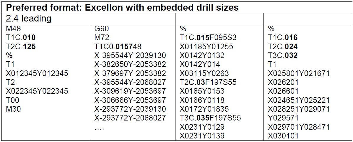
3. If your system generates drill files with the drill diameters embedded at the top of the drill file, then a drill tool
report file is not required to be included within the zip file. Otherwise a drill tool report file is required. All NC Drill
files should be exported in no less than 2.4 decimal coordinate placement. Drill files that have a smaller decimal
format or a format that does not match the Gerber decimal format may suffer pad misalignment and then annular
ring errors will be reported back to you.
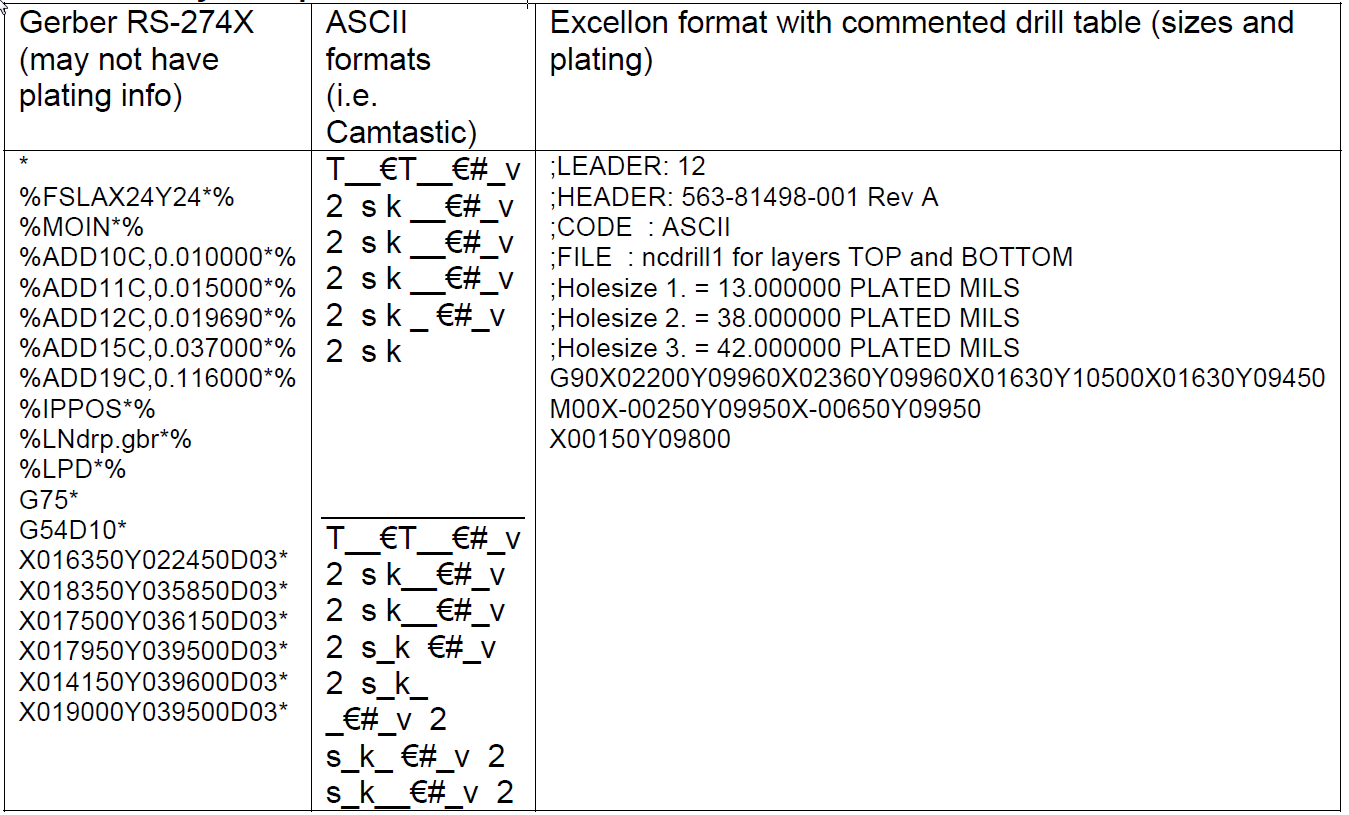
Some drill file examples below (as viewed in a text viewer):

Occasionally Acceptable formats:

Occasionally Acceptable: Excellon format with a separate drill file (table)

Multiple via drill diameters that have their pads covered in soldermask will report as errors because the software
does not know if you want all your vias covered (tented) or not. You can either clear soldermask from (give relief
to) the via pads, or ignore this error.
5. Fabrication drawings with detailed information for Slots, cutouts, and outlines will not appear in your output
when they are uploaded as other. If you desire to see the shape or outer contour of your PCB and any internal
cutouts, you can include these outlines on your solder mask layers for visual reference during your Free DFM
image plot review. All files from Free DFM are viewed from the topside of the board, through the board.
The bottom side silkscreen text should look backwards for it to read correctly when viewed from the bottom.
6. If your board outline is on a separate layer and uploaded to other, it will not be shown on the Free DFM output,
not will tests be run using your outline. Please note: If exposed copper is not desired on the board edge, then
copper should be kept 10 mils away from outline rout edge by outer layers and 15 mils for inner layers. For
scoring keep copper 15 mils away for outer layers and 20 mils for inner layers. Please also note: If an outline is
not included in one of your uploaded layers, and an order is placed without one, the job will go on hold until one is
provided. The GKO (keep out) layers can only be used as the board outline if it is clearly indicated that we can do
so.
7. Free DFM tests are designed for standard and custom specification orders, and it will not flag errors that may
occur if the job is ordered as any other type. For instance the copper to copper spacings (trace and space) for
other order types differ from what is allowed on standard and custom spec orders. A 33 special order is allowed a
minimum trace and space of 6 mils for 1 oz copper, but Free DFM will not flag trace and spacings between 5 and
6 mils.
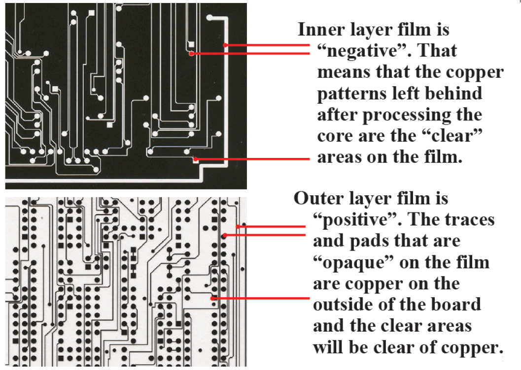
8. When selecting the image polarity of a layer, then like a photograph, choose positive if your inner layer is
viewed literal and negative if it is the opposite of where copper should be.
9. When assigning inner layer polarity on the Free DFM system, one needs to know if the inner layers are drawn
with traces or filled with copper pour and or even both. This type of layer is a positive image. It will look just like
an outer layer.
The reverse and or negative polarity is when the inner layer is a power or ground flashed plane with anti pads for
drill clearance and flashed thermal spoke wheel pads for inner layer drill connection. Incorrectly assigning the
inner layer polarity will result in erroneous error reports.

For more details on the Free DFM, please click here.
