
- PCB Engineering
- CAM Procedures
- Gerber File
- Gerber Generation
- Pick&Place Generation
- DFM Check Item
- DFM Check Details
- PCB FAB Tutorial
- Finished Surface
- Impedance Apply
- Impedance Type
- PCB Laminates|Stackup
- Stackup with Impedance
- Capabilities
- Tolerances
- Material Comparison Chart
- Rogers Matierl datasheets
- Rogers Material Choose
- Avoid missing Feature
- HDI PCB Stackup
Free DFM Check
As a value-added option for our Assembly services, we offer Free PCB File Check, also known as Free DFM,
namely we help check your PCB design file for possible issues that may affect manufacturability. If any issues
were detected, we would get in touch immediately to solve the issue together, then schedule the PCB production
accordingly.
The DFM will be carried out from 5 aspects: Drill Checks, Signal and Mixed Layer Checks, Power/Ground Checks,
Solder Mask Checks, Silkscreen Checks. Read through the following paragraphs for more details.
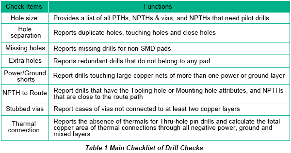
1. Drill Checks
The Drill Checks action is intended to find potential manufacturability defects in drill layers (through, buried and
blind via layers) and generate statistics on drill layers. It is intended to operate only on drill layers. It uses the drill
layer, the top and bottom layers of its drill stack and any power or ground layer in the stack. The main checklist is
displayed in the following Table 1.
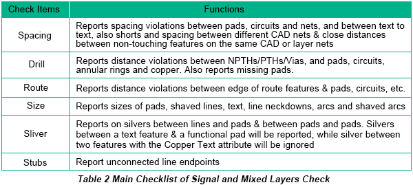
2. Signal and Mixed Layer Checks
This function is intended to find potential manufacturability defects in Signal layers and mixed layers and
generate statistics. The action can operate on any layer, but is mainly intended for signal layers. It uses the layer
itself and any NC (drill or route) layer which pierces it. The main checklist
is displayed in the following Table 2.
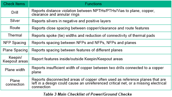
3. Power/Ground Checks
The Power/Ground Checks are intended to find potential manufacturability defects in power, ground and mixed
layers. It uses different algorithms to diagnose negative and positive power and ground layers. The main checklist
is displayed in the following Table 3.
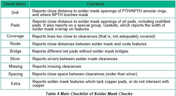
4. Solder Mask Checks
This function checks Solder Mask layers for potential manufacturability defects. Solder Mask layers are always
assumed to be negative, that is, all positive features describe clearance or the absence of solder masks. This
action also checks if solder paste has been deposited on all SMD pads. The action operates on a single Solder
Mask layer per side at a time. If more than one SMD is selected, the action will not work. The main checklist is
displayed
in the following Table 4.
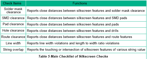
5. Silkscreen Checks
This function is intended to find potential manufacturing defects in silkscreen layers and generate statistics. The
check operates only on silk screen layers because it relies on the job matrix to find the related external copper,
solder mask and drill layers against which to check. The main checklist
is displayed in the following Table 5.
Wanna take advantage of our Free DFM option? Start from sending a quote request for your custom
PCB Assembly project to [email protected]. Make sure you include your PCB design file, BOM and other
specific requirements. Our agents will check your file and give a custom quotation within 1-2 working days.
