
- PCB Engineering
- CAM Procedures
- Gerber File
- Gerber Generation
- Pick&Place Generation
- DFM Check Item
- DFM Check Details
- PCB FAB Tutorial
- Finished Surface
- Impedance Apply
- Impedance Type
- PCB Laminates|Stackup
- Stackup with Impedance
- Capabilities
- Tolerances
- Material Comparison Chart
- Rogers Matierl datasheets
- Rogers Material Choose
- Avoid missing Feature
- HDI PCB Stackup
1.Board cutting
cut the whole sheet of CCL into small panel according to the array drawing of MI, then to grinder the edges and
bake them according to the manufacture instruction.

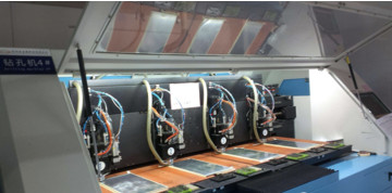
2.Drilling
To form a path for component installation and electric conductivity among PCB layers.
3. PTH
(Chemical Copper) Create a continuous copper layer in hole.

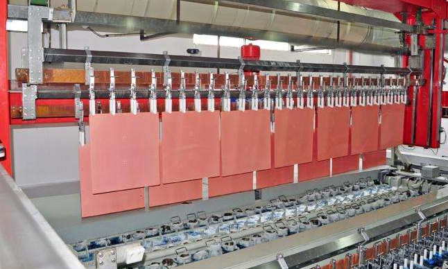
4.Panel Plating
Apply plating after PTH to avoid no copper in hole after micro-etch. Baking after plating for better
stock;
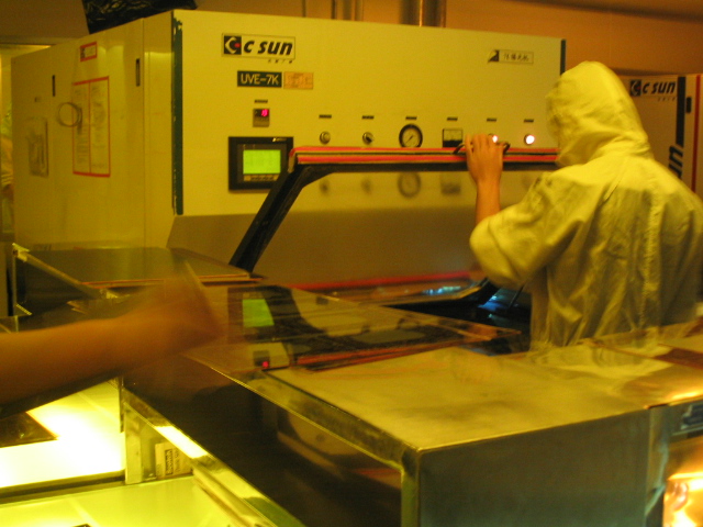
5. Outer Dry film(ODF)
Laminate dry film on clean Cu cover through hot-pressing, then transfer circuit patter artwork onto dry film by
Exposure and developing.
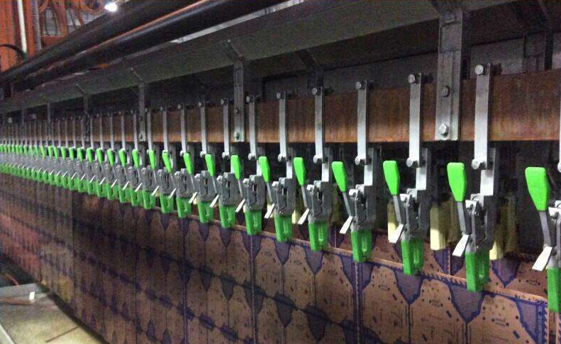
6. Pattern plating
Plating Cu on conductor pattern (Plating a layer Cu on circuit patterns to increase reliability of PCB
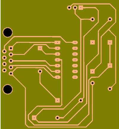
7. Outer Etching
Remove non-required copper with etching solution to obtain pattern required.
8. Outer AOI
Scan the conductor layers with any short, open, nicks,
pits. Dents. Etc.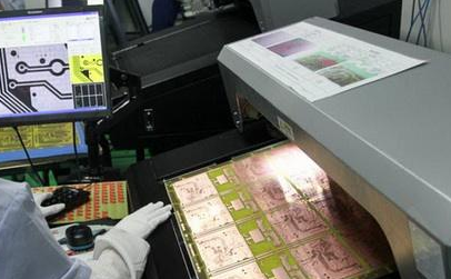
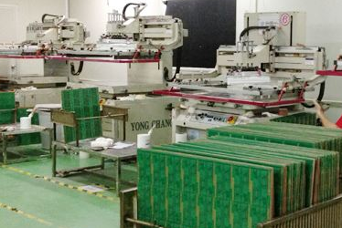
9.Solder mask
1). Choose the correct grinding way so as to make out a clean board surface;
2). Select regulated ink with appropriate viscosity; Accurate 1st stage baking;
3). Select the appropriate exposure/imaging
10.Finished
surface
To create one coat over the outer copper surface, the type has HASL Lead free, HASL, Immersion gold,
Immersion Tin, OSP and so on.

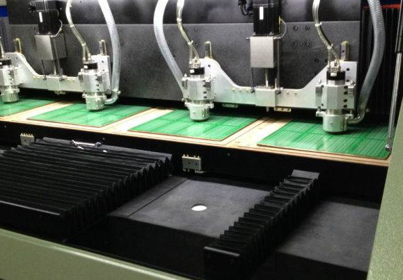
11.Routing
To uses digital control routing machine to process outline according to customers' specification
12.E-Test(Open/short)
using test fixture to electrical function of productions
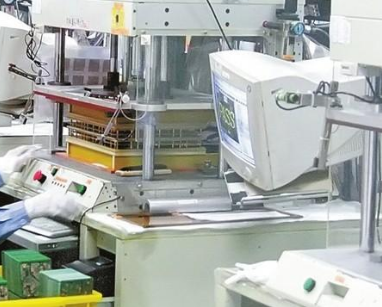
13.FQC
Visual inspection was according to specification of customer, and prevent rejected boards from flow out.
Cleanliness test: Put board into solvent then test Cl-
content through OMEGA 600SMD tester.
14.FQA
Visual
inspection was according to specification of customer, and prevent rejected
boards from flow out
15. FGC
to prevent F.G being broken during transporting packing them according to customer's requirements
16. Packing/shipping
Follow customer's requirement to pack PCB.
Shipping: According to requirement of PO to ship out.
KINGRON have the rich experience on full service PCB fabrication, we provide the quick turn around lead time and
